
产品资讯


超高速信号设计,高端网络平台中的创新与应用
发表时间:2019-05-15 00:00:00
随着5G时代的到来,电信革命正以前所未有的规模快速发展。海量数据及其所需的数据流容量推动了新一代高速宽带网络设备的诞生。高速信号完整性是设计高速网络平台的主要挑战之一,高速印制电路板的插入损耗、VIA效应和SSN(同步开关噪声)如何被最小化和可控制,是完善通信设备性能的关键。鉴于这一必要性,NEXCOM、ITRI(工业技术研究所)、FHT(First Hi-Tec)和TUC(台湾联合技术公司)合作开发新技术,以克服高速信令的挑战。
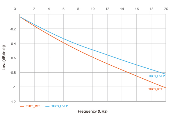
Figure 1. TUC3 correlation of signal speed and insertion loss.
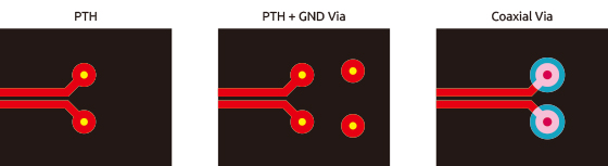
四方联合共同推出了一种新型的“超低损耗”材料,称为Tuc3,其插入损耗可以达到-0.57db/inch@25Gbps(图1)。另一个被称为同轴VIA(如图2所示,同轴VIA架构)的创新技术,它在信号模拟方面表现出色,其中SDD21指数分别为-0.2db@8GHz、-0.3db@12.5GHz和-1.2db@28GHz,而同一指数通过传统的PTH VIA读取0.3db@8GHz、0.5db@12.5GHz和1.6db@28GHz(图3)。在同轴via与pth(电镀通孔)或pth+gnd via的对比图中,我们发现传输速度越高,性能和信号完整性的差异就越大(表1)。在电路板布局中采用同轴通孔,可以在高速信号时保持信号的完整性。
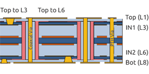
Figure 2. Coaxial VIA stack-up.
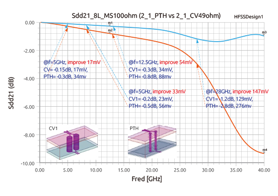
Figure 3. Simulation of Coaxial VIA vs PTH@Sdd21 across different speeds.
Simulation Improvement (mV) | Signal Measurement + Improvement (mv) | |||||||||
CV1 | PTH | Intel GND Via | Coaxial Via 1 | Coaxial Via 2 | Coaxial Via 3 | |||||
@10Gbps | 17 | 381 | 396 | 15 | 397 | 16 | 400 | 19 | 402 | 21 |
@16Gbps | 33 | 336 | 352 | 16 | 355 | 19 | 356 | 20 | 356 | 20 |
@25Gbps | 54 | 199 | 222 | 23 | 269 | 70 | 281 | 82 | 284 | 85 |
Table 1. Signal measurement of types of VIA @ different speeds.
该团队带来的第三个创新是如图4所示的嵌入式电容器(红色路径)分层在PCB FAB中,与目前主流的SMD型电容器(绿色路径)相比,将电路轨迹减少50%,从而大大提高了信号完整性,因为它减少了高速IC芯片(如Mellanox ConnectX-5等)产生的大部分SSN。(图5)展示了带嵌入式电容器的PCB FAB,其容量为0.01uf@8GHz,电阻为@6 ohm。
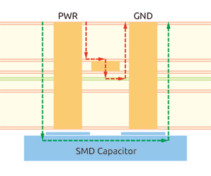
Figure 4. Trace length-embedded capacitor (red) vs SMD capacitor (green).
Figure 5. Cross Section, PCB FAB with embedded capacitors.
新汉开发的100G LAN模块,展示了合作开发整合的三项创新(图6)。LAN模块支持2 x100G QSFP28中的100G控制器。端口0的设计遵循100G IC制造商的设计指南,采用PTH+GMD VIA和符合3“长度限制的高速信号电路;同时,端口1的设计基于以上3种创新技术,从而允许高速信号将长度延长至14”(图7)。在验证IEEE一致性测试的过程中,100G LAN模块的端口1 QSFP28完全符合IEEE802.3BM的要求,如图所示(图8)。
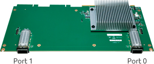
Figure 6. 100G LAN module snapshot.
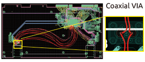
Figure 7. 100G LAN module PCB layout.
npoc240 | Port No. | Eye Height (95mV) | Eye width (17.84ps) | Jitter | Pass/Fail | |
TUC-3, 14inch Port 0 (14") | Sample A | TX1 | 142 | 20 | 18.7 | PASS |
TX2 | 117 | 19.6 | 18.6 | PASS | ||
TX3 | 142.6 | 22.1 | 17.3 | PASS | ||
TX4 | 129.8 | 21 | 17.3 | PASS | ||
Sample B | TX1 | 176.6 | 18.4 | 18.1 | PASS | |
TX2 | 140.4 | 20.7 | 20.1 | PASS | ||
TX3 | 189.4 | 22.4 | 16.8 | PASS | ||
TX4 | 175.5 | 20.5 | 16.7 | PASS | ||
Sample C | TX1 | 158.1 | 22.1 | 15.5 | PASS | |
TX2 | 155.3 | 18.5 | 19.9 | PASS | ||
TX3 | 170.2 | 22.1 | 17.7 | PASS | ||
TX4 | 136.2 | 18.1 | 16.7 | PASS | ||
Average | 153.6 | 20.4 | 17.8 | PASS | ||
Figure 8. Readings of eye diagram, port 1, 100G LAN module.
此卡安装在基于Intel Purley平台的新汉 NSA 7146中,并在新汉自己的DPDK下运行时,我们见证了令人印象深刻的吞吐量数据(表2)。我们在不增加中继器、定时器和任何其他活动组件的情况下实现这一点,以保护其信号完整性并保持所需的性能。这个100G LAN模块标志着一个里程碑,是高速信号设计的真正突破。
Frame Size | Throughput | % 100gb/s |
512B | 1,330,474,624/1,255,701,950 | 94.38 |
1024B | 718,385,872/718,385,872 | 100 |
1280B | 576,907,231/576,907,231 | 100 |
1518B | 487,646,294/487,646,294 | 100 |
Table 2. Throughput, port 1, 100G LAN module.
![]()
Copyright © 2011-2023 北京兴汉网际股份有限公司

